All Samsung’s global semiconductor manufacturing facilities certified for reducing carbon emissions
Samsung Electronics has received the semiconductor industry’s first “Triple Standard” for carbon, water and waste by Carbon Trust, the company said on June 3.
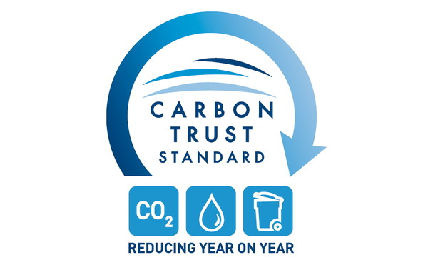
Samsung was awarded this certification by reducing the amount of carbon emissions, water use, and waste discharge over the past three years at five operations --Giheung, Hwaseong, Pyeongtaek, Onyang and Cheonan factories in Korea and four global manufacturing sites in U.S. and China (Austin, Suzhou, Tianjin and Xi’an).
This is a huge feat, considering that it is extremely challenging for semiconductor manufacturing companies to meet all three qualifications at once.
“For decades, Samsung has been striving to incorporate environmental sustainability into every aspect of the semiconductor manufacturing process,” said Jang Seong-dai, senior vice president and head of DS Corporate Sustainability Management Office at Samsung Electronics.
Jang added, “We’ll continue to pursue more environmentally sustainable policies across the entire production and supply chain.”
Samsung has been making various efforts in carbon reduction, water resource conservation and recycling, and has been managing these as important sustainability goals.
Samsung Electronics strives to incorporate environmental sustainability into everything it does. Samsung’s products are thoughtfully designed to minimize the impact on the environment during their entire lifecycle – from planning and manufacturing to consumption and recycling.